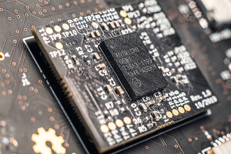
GEM1 Adapter
This repository contains PCB design files for an adapter board accommodating the GEM1 chip created jointly by zGlue and Antmicro. The GEM1 design utilizes the zGlue ZiP chiplet technology and has been prepared using zGlue's ChipBuilder tool. The design has been produced as a single integrated circuit in the LGA-96 package.
Languages
GEM1 Adapter
Copyright (c) 2020 Antmicro
This repository contains PCB design files for an adapter board accommodating the GEM1 chip created jointly by zGlue and Antmicro. The GEM1 design utilizes the zGlue ZiP chiplet technology and has been prepared using zGlue's ChipBuilder tool. The design has been produced as a single integrated circuit in the LGA-96 package.
The GEM1 chip contains the following components located on a dynamically reconfigurable interposer:
- 2x Lattice
ICE40UP5K-UWG30ITRFPGAs used for processing and system control - 32Mbit SPI FLASH memory
- 10-channel DPDT MIPI switch allowing to connect a 2-lane MIPI CSI-2 interface either to the processing FPGA or to external output (pass-through mode)
- 12MHz system clock generator
- Internal LDOs and power management unit providing 1V2, 1V8, 2V5, 3V3 voltages
Power is supplied to the chip from a single VUSB voltage of 5 VDC. The
actual configuration of the system running inside the GEM1 zip depends
on the configuration routing file that is uploaded to the Smart fabric
interposer. Also, pin functions of the LGA package may vary depending on
the uploaded routing file. The board break-routes signals for the MIPI
CSI-2 interfaces (Input and Output), along with the internal flash and
FPGA configuration interfaces, control signals and power supplies.
Relevant projects
Nothing found
Apologies, but no results were found.
